
Precision Temperature Control: Eliminating Micro-Defects in Lithography and Etching
Why ±0.1°C stability is non-negotiable for sub-7nm lithography and high-aspect-ratio etching
In sub-7nm process nodes, thermal variations greater than ±0.1°C can result in stark dimensional changes. This is due to photochemical responses to EUV lithography. Studies have shown that thermal variations of 0.1°C can result in an approximate 0.15nm increase in dimensions (Case studies on Thermal Engineering, 2023). High aspect ratio etching instabilities can lead to inconsistent wall angles, which increases via resistance by approximately 18% and reduces yield by 3-5% per wafer. This explains why most manufacturers have begun adopting dual circuit chillers for semiconductors. These dual loop systems have independent refrigerant circuits that absorb thermal shocks from separate process tools. These systems are markedly better than traditional single circuit systems, which suffer from large thermal swings due to sudden changes in tool load. This is especially important for sub-7nm processing, where extremely tall, high aspect ratio structures (100:1) are being created. Normal thermal delays can cause significant taper on the wafer.
How thermal drift causes photoresist scumming, line-edge roughness, and overlay errors
Thermal drift and photoresist exposure trigger these three correlated failure modes:
1. Scumming: Undeveloped residues are left behind in 12nm trenches when cooling rates are uncontrolled and drops below 0.1°C/sec
2. Line-edge roughness (LER): In post exposure bake, roughness increases by 40% with temperatures swings >0.3°C (Precis. Eng. 2017)
3. Overlay errors: For every 0.1°C shift, differential expansion in silicon wafer and reticles causes 0.25nm misalignment
These defects collectively account to 62% of parametric yield loss in 5nm nodes. With dual-circuit chillers ensuring thermal zone cross-contamination containment, etching chambers can stay at ±0.05°C stability while lithography tools are at freely determined setpoints.
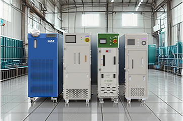
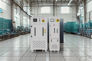
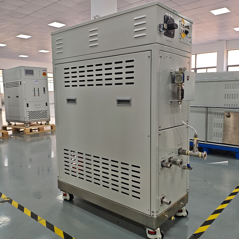
Independent Dual-Circuit Cooling: Enabling Simultaneous Multi-Process Support
Cooling distinct tools—e.g., 12°C wafer scrubbers and 65°C rapid thermal processors—without cross-channel interference
Managing extreme temperature differences is very crucial in modern semiconductor manufacturing. While wafer scrubbers need to work at around 12 degrees Celsius to prevent wafer contamination, rapid thermal processors must work at 65 degrees Celsius to properly activate dopants. Due to temperature differences, standard chillers, with only 1 circuit, run into problems where ''cold'' parts absorb heat from the ''hot'' processes, leading to a rapid temperature change of plus or minus 3 to 5 degrees. Hence, dual circuit chillers are increasingly becoming a necessity. Dual circuit chillers refrigerate piping completely, allowing complete separation of refrigerants. Each side contains its own compressor and controls. One side keeps scrubbers at 12.2 degrees Celsius, while the other keeps RTP tools at 65.3 degrees Celsius. This refrigeration separation almost completely stops unwanted energy transfer between circuits. This results in fewer problems with insufficient resist stripping in the scrubbers and better dopant activation uniformity in the RTP. As reported in Semiconductor Engineering last year, this method has improved tool utilization by ~ 22 % and alleviated yield issues associated with the simultaneous running of multiple processes.
Let's Chill With No Interruption
Semiconductors are designed to be heat sensitive. We cool them carefully to avoid changes in temperature where we need to hold only to ± 0.1°C. To take temperature control maintainance circuits, one at a time, the dual circuit chillers allow circuits the system to seamlessly switch between each other to control temperature. Thousands of dollars worth of wafer losses are preserved. Even the maintenance we need to do to cause them to stop chillers, such as fefill, pump repair, etc. Won’t cause production disruption. For connections lithography which needed only minor temperature shifts are needed, this protection is very critical.
Why do dual circuit semiconductor chillers lead to a marked reduction in MTTR compared to previous generations of single circuit systems?
Because of independent cooling circuits, maintenance teams can address issues in some regions or areas without a complete system shutdown, resulting in almost a 40% reduction in Mean Time To Repair (MTTR). This is in stark contrast to older single circuit designs. Troubleshooting is done in a fraction of the time (approx 66% faster). When addressing a failure, technicians are dedicated to that particular faulted circuit while the rest of the system continues to operate at its required set point. To address failures in older systems, even minor maintenance required the system to be fully shut down. The parallel circuit design offers operators three key advantages aimed at maximizing uptime:
- The ability to perform maintenance while the system is operating
- Modular structure of the system components
- Clear zoning to quickly identify issues
This design optimizes uptime and overall system effectiveness. OEE is impacted positively since maintenance tasks that typically lead to system shutdown, such as compressor replacement and coil cleaning, are performed.
Total Cost of Ownership and Yield Impact: Calculating the ROI of Dual Circuit Semiconductor Chillers
The initial purchase price of single circuit chillers may be lower, but from every standpoint, dual circuit semiconductor chillers end up being less expensive due to operational savings and the protection of production yields. The built-in redundancy protects the chillers from damaging temperature excursions. According to a report in Semiconductor Digest last year, just one hour of temperature drift during the etching process can destroy $740,000 in wafers. Besides the operational savings, maintenance costs are lower as well. Facilities Engineering Journal reported in 2023 that systems of this kind require 41% less maintenance. There is a 30% reduction in the temperature-related rework and hence an increase in the operational efficiency of 30% due to a reduction in energy waste caused by temperature-related rework. Many manufacturers, when taking all the above Factors into account, estimate that their total cost of ownership over a five-year period is, on average, 18% lower than previous models. What is most remarkable is that it is the speed at which they pay back the initial investment that really stands apart. Many high volume fabrication plants experience a payback on their investment in as little as 14 to 26 months due to the 22% increase in Overall Equipment Effectiveness.
FAQ
Why is ±0.1°C temperature stability critical in semiconductor manufacturing?
Sub-7nm lithography and high-aspect-ratio etching processes are extremely sensitive, and very little thermal variation can lead to dimensional and structural imperfections, which are yield and performance detractors.
How do dual circuit chillers enhance semiconductor manufacturing?
Enhanced precision temperature control and lower maintenance challenges are made possible by dual circuit chillers thermal contamination avoidance as a result of independent cooling circuits.
What are the cost benefits of dual circuit chillers?
The costs of dual circuit chillers are justified by the savings due to improved energy efficiency, lower maintenance costs, protection against yield losses due to temperatures fluctuations, and a quick return on investment.