
The subtleties of Thermal Stability for Sub-7nm Photolithography and EUV Devices.
To build semiconductor structures smaller than 7nm, it is necessary to be able to control and manage a level of heat variability that is almost unattainable. Extreme Ultraviolet (EUV) lithography systems are required to work at temperature stable to ± 0.01°C. This is equivalent to stabilizing the temperature of an entire swimming pool at a level of ±0.0005°C. At extreme small dimensions, temperature variations lead to lens materials and wafer stages to thermally expand and contract, leading to (a) deviations from the predetermined layout (the highly precise light paths that are required to expose a small feature) and (b) collapses of the light paths. Such challenges are encountered by immersion lithography as well. A mere 0.1°C temperature variation leads to fluidic refractive index variations. Furthermore, it leads to an out of focus state of the patterns. It is a relentless and, in fact, the most significant fact to consider in relation to the new EUV power modules that have a power density greater than 500kW/ m2. If heat is not stable to a high degree of precision, the primary aim of nanometer-scale manufacturing will be achievable, yet defective, electronic components.
Technological Impacts of Chiller-Induced Thermal Drift on Overlay Accuracy in Semiconductor Manufacturing
Chiller systems in semiconductor manufacturing have a unique effect on overlay accuracy, the precision with which multiple layers of silicon are aligned. The temperature of these chillers affects the wafers in a way that each thermal induced degree of the chillers cause the silicon wafers to expand with rates of up to 2.6μm/m. At 300 mm wafer diameters, the expansion can lead to up to 3 nm of out of alignment wafers. Advanced 5 nm chip manufacturing processes can only tolerate 1.7 nm of out of alignment wafer layers. It is also important to highlight the effect that the thermal drifts have on the lithography stage of the equipment. The drifts, as engineers put it, have a causing effect on the “mechanical creep” of the use of the lithography equipment causing the already hypothetically small positioning inaccuracies of the equipment to be larger and larger from use.
When layers misalignment occurs, serious problems can be created such as short-circuiting or gaps in the circuitry. Such defects result in manufacturers losing approximately $740,000 every hour (Ponemon Institute, 2023). Advanced modern chillers have smart load management and can maintain temperature stability to within +/- 0.005 degrees Celsius. This allows the semiconductors to be manufactured with the critical +/- 0.15 nm accuracy required to achieve good yields.
Standards for Cleanrooms and Fluid Purity in Semiconductors
Fluid Path Integrity and Particle Control
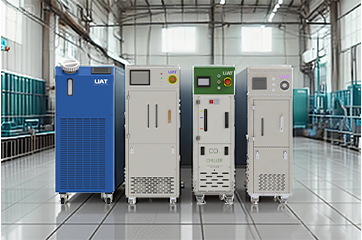
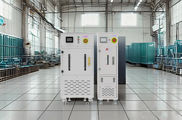
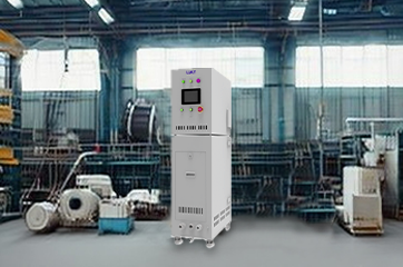
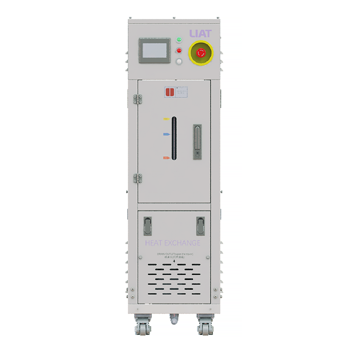
Chillers used in cooling systems for semiconductor fabrication plants must be kept to ISO Class 1-4 standards so as not to compromise extreme ultraviolet lithography (EUV) and other stages of manufacturing. Any airborne contaminant greater than 0.1 microns would be problematic for targeting ultra small sub-5 nanometer wafers. Modern chiller systems have fully sealed refrigerant pathways and use high grade stainless steel construction similar to that of surgical instruments to minimize contamination. These chillers use advanced molecular contamination filters as well as HEPA filters to ensure that positive differential pressure and airborne contaminants are kept to less than 1 per cubic meter at 0.1 micron. These extreme measures ensure that ASML lithography machines are not affected by contaminants that would degrade the lithography machines' optics. The defect rate of wafers is controlled to below 0.01 per square centimeter. These machines cost over two million dollars and are highly sensitive to optical deposition.
Selection of Corrosion-Resistant Materials and Deionized Water Compliance (≥18.2 MΩ·cm)
Semiconductor fab cooling chillers must provide ultrapure water (UPW) systems with all thermal transfer points >18.2 MΩ·cm resistivity (i.e. >99.999999% of ionic contaminants). Standard industrial chillers do not work here because of galvanic corrosion in copper-nickel alloys that release metals into the coolant loops. As a result, next-gen solutions are designed with:
- Electropolished 316L/904L stainless steel fluid circuits.
- Passivation layers that don’t shed iron oxide.
- Non-metalic (Kalrez® FFKM) seals that withstand thermal cycling.
This design prevents resistivity drops to <18.0 MΩ·cm that cause wafer hazing—a $740k/incident defect (SEMI Benchmark Report, Yield Loss Drivers in Advanced Node Fabrication, 2023). Compared to pharmaceutical-grade systems, semiconductor chillers must also tolerate permeation of etch chemicals, such as HF, through equipment interface.
Boosting Equipment Lifespan and Yield Improvement using Trustworthy Semiconductor Fab Cooling Chillers
Evaluating Yield Loss: ± 0.3°C Flaw and Its Association with Defects (SEMI F47)
There are a lot of reasons, such as defect concentration, for keeping a semiconductor fab at a constant temperature. Defects are killer and, according to the semiconductor industry's defect management strategy, SEMI F47 (draft), eliminating defects is a strong motivator. If a fab does not meet SEMI F47 standards, it will produce 1.5-3% fewer chips per 100 wafers due to killer defects. All the wasted silicon is a big financial loss for a fab, but the real cost of fluctuating thermal conditions is equipment wear and the associated increase in maintenance costs. Equipment, like extreme ultraviolet (EUV) lasers and etch chambers, are particularly sensitive to thermal cycles, and are prone to a phenomenon called thermal fatigue which leads to a 18% increase in maintenance costs and downtime.
This is why modern fabrication plants spend money on cooling systems that can keep temperatures within a range of plus or minus 0.05 degrees Celsius. Such precision prevents failures, protects millions of dollars worth of equipment, and provides consistent production levels that factory managers need to support healthy profits.
Right-Sizing and Customizing Industrial Chillers for Dynamic Process Loads
When cooling a semiconductor fabrication facility, the thermal requirements differ. Chill cooling needs to be right-sized, customized, or all sorts of problems will occur. Big chillers will circle on and off too much and over time will waste power and burn out the components that start and stop too frequently. Small ones cannot keep a critical +/- 0.3 degree range when demand spikes. This causes critical chips being produced to fluctuate, and as we know, temperature is a major quality factor. To combat this, custom built systems and smart PID control technology adjust cooling levels as conditions shift. Pairing smart PID controls with special phase change materials as thermal shock absorbers, engineers have the right combination to minimize defects and save energy. Customers track savings of 25 to 30 percent, compared with the standard fixed capacity chillers.
FAQs
Why is thermal stability vital in semiconductor fabrication?
Temperature stability is essential in semiconductor fabrication because temperature variations can lead to an imprecise semiconductor fabrication process, resulting in defective and poorly functioning components.
What are the consequences of thermal drift caused by chillers?
Thermal drift caused by chillers can lead to the misalignment of silicon layers. This in turn can lead to silico n short circuit defects and increased production costs due to production delays.
In what way do modern chillers help to achieve cleanroom and fluid purity standards?
Modern chillers help achieve cleanroom standards through the use of sealed refrigerant pathways and anti-corrosive materials that do not allow for contamination, preserving the integrity of the chip.
Table of Contents
- The subtleties of Thermal Stability for Sub-7nm Photolithography and EUV Devices.
- Technological Impacts of Chiller-Induced Thermal Drift on Overlay Accuracy in Semiconductor Manufacturing
- Fluid Path Integrity and Particle Control
- Boosting Equipment Lifespan and Yield Improvement using Trustworthy Semiconductor Fab Cooling Chillers
- Right-Sizing and Customizing Industrial Chillers for Dynamic Process Loads
- FAQs